about the system protection unit in ADSP-SC59x
The system protection unit (SPU) is being used/designed to avoid conflicts when having multiple processors with shared peripherals. It actually behaves like semaphores to lock a memory region (all peripherals are actually memory regions, called MMR).
The SPU provides:
- write protection from system and core requesters
- lock multiple peripheral configuration registers over a global lock mechanism
- write protect for its own write protection registers
- security privileges to peripherals and system resources
- protect secure peripherals from non-secure requests
It stands between System Crossbar (SCB) which is the main bus interconnect fabric and SMMR (System Memory Mapped Registers).
For example:
┌─────────┐     ┌─────────┐     ┌──────┐     ┌─────────┐
│ ARM A55 │────>│  SCB0   │────>│ SPU  │────>│  UART0  │
└─────────┘     │ Crossbar│     │      │     │  SMMRs  │
                └─────────┘     └──────┘     └─────────┘
                                    ▲
                                    │
                        Checks SPU_WP[n] and
                        SPU_SECUREP[n] before
                        allowing write/access
The SPU gates any MMR access to any peripheral from any requester that comes through the SCB. Depending on the configuration of the write-protection registers in the SPU, the SPU does or does not allow the MMR write to go through.
The SPU also checks whether the transaction is a secure or non-secure transaction and blocks it according to the configured security setting for the target destination. A secure requester can generate secure read or secure write transactions which can access secure or non-secure completers. A non-secure requester can generate non-secure read or non-secure write transactions and can only access non-secure completers
Functional Description
We have set of registers as:
- SPU_CTL (Control Register)
- SPU_SECURECHK (Secure Check Register)
- SPU_SECURECTL (Secure Control Register)
- SPU SECUREC[n] (Secure Core Registers)
- SPU_SECUREP[n] (Secure Peripheral Registers)
- SPU_STAT (Status Register)
- SPU_WP[n] (Write Protect Registers)
So the protection can be examined under two categories. Global locak which protects confiuguration registers and write protect register lock which protects the write protect register (SPU_WP)
!! We also have one interrupt as SPU0_INT to handle errors or unpriveleged accesses.
About the Write Protect Register Lock (SPU_WP)
We have one instance of this register for each peripheral as can be seen in the figure below.
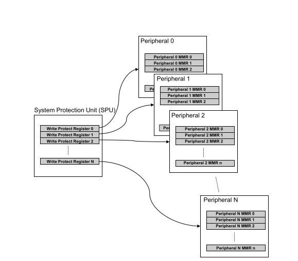
The mechanism is that when we set the bits, SPU locks the corresponding requesters from accessing that register address space.
Important note: When the SPU initializes the write-protection register, any writes that are in-progress complete before the SPU blocks subsequent writes.
If we lock everyone’s access to the peripheral to only way to get back is the system reset.
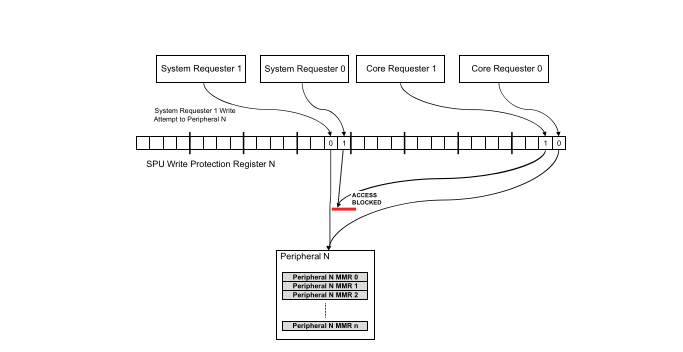
The SPU_WP is actually kind of interesting for me beacuse there is adistinction between the system requesters and core requesters. The register has two fields as .SM (System Requester x Write Protect Enable) and .CM (Core Requester x Write Protect Enable).
The requesters are acutally the bus masters that can initiate writes to peripheral registers (SMMRs). Core requesters, as understood, refers to all cores (ARM, SHARC) we have. Its a 3 bit field since we have one ARM and two SHARC cores. For the system requesters, there is no information on the 59x (ADSP-SC595/SC596/SC598 and ADSP-21593/21594/ADSP-SC592/SC594) Processor Hardware References. However, on the SC573 documentation, it says:
| Bit 16 (.SM[0]) -> | DBG (Debug subsystem) |
| Bit 17 (.SM[1]) -> | ETR (Embedded Trace Router) |
| Bit 18 (.SM[2]) -> | Enhanced Bandwidth MDMA |
About the Global Lock Configuration
SPU has the capability of handling global locks. They are controlled over SPU_CTL register. By setting the .GLCK (stands for Global Lock) to a value rather than 0xAD, a system wide lock is active.
For the some peripherals, we have lock enable bit in their own control registers. When this bit is set the peripheral can be notified about the global lock signal and blocks accesses to its own control register.
The Peripherals with global lock bit in their MMR:
- General-Purpose IO (GPIO)
- System Event Controller (SEC0)
- Trigger Routing Unit (TRU0)
- Clock Generation Unit (CGU0)
- Clock Generation Unit1 (CGU1)
- Clock Distribution Unit (CDU0)
- Dynamic Power Management (DPM)
- Reset Control Unit (RCU0)
- System Protection Unit (SPU0)
- L2 Memory Controller (L2CTL0)
This can be examined from the figure below:
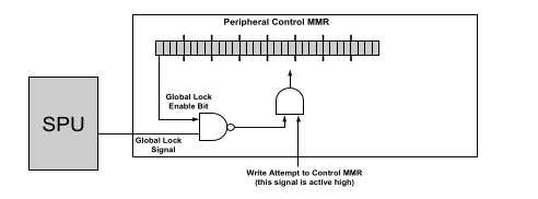
SPU can also protect its own control registers as we mentioned.
We use .WPLCK (stands for Write Protect Register Lock) FROM SPU_CTL register.
When both .WPLCK set and the global lock is enabled, SPU blocks the access to their own write-protection configuration registers. So, one need to disable global lock first to be able to enable write access to write-protectionr registers.
Handling the unpriveleged accesses
If any write attempt happens to a locked MMR peripheral, SPU blocks the write and generates a bus error to the requester. Requester (the cores or systems) can deal with that error by themselves.
As we said SPU can also lock its registers. If someone tries to access these locked registers, SPU blocks it and records this as error in .LWERR (Lock Write Error) bit on SPU_STAT register.
On the SPU side, we have one interrupt line named SPU_INT.
We can use it to catch
- write protection violation
- security violation
For the write protection violation, we can set .PINTEN (Protection Violation Interrupt Enable.) bit in SPU_CTL register.
For the security violation, we can set .SINTEN (Secure Violation Interrupt Enable) bit in the SPU_SECURECTL register.
!! For both of the events, if we get the interrupt, the .VIRQ (Violation Interrupt Request) bit in SPU_STAT register is being set.
One important point is that when global lock + peripheral locks its configuration register state exists, if someone tries to access that peripheral, peripheral itself blocks it and reports the failed attempt. The SPU itself can not be aware of that situation so does not provide any information to us.
!! If the global lock exits but perihperal not locked itself, we can still access to that peripheral.
For the sake of ‘security’
For the security of cores, we have SPU_SECUREC registers for each DSP (SHARC) cores in the system. For the peripherals, we have SPU_SECUREP registers.
SPU_SECUREC
We can control the non-secure accesses over this register. It is just one field as .CSEC (Core Secure) and it controls the accesses between that core and L1 memory. If its enabled only secure accesses are allowed.
SPU_SECUREP
We control the perihperals over this. There are multiple instances of that register that are belong to specific MMR range (simply each of them is belongs to one peripheral).
There are two field to control, one is .MSEC (Requester Secure Enable). When this set, perihperal generates secure transactions as requester and vice-versa.
The other field is .SSEC (Complete Secure Enable). When this set, only secure transactions are allowed to access that peripheral and when its clear, the status of transactions is ignored.
References: